Layout Pcb Power Amplifier
It’s unlike any other power amplifier from that era. Also, we have top and experienced pcb engineers in our pcb manufacturing and assembling firm based in china.
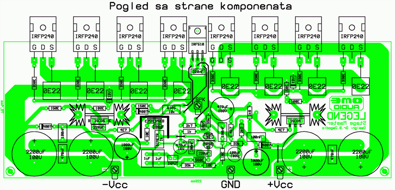
250W RMS Power Amplifier Legend Stage Master Circuit Scheme
And ever since, we have grown to be reckoned with in the pcb assembly industry.

Layout pcb power amplifier. Low power audio amplifier using bc109c along with bd679 and bd680 darlington pairs: This isn’t as hard as it might sound. On the second stage of the circuit, q1 and q2, which are mpsa43 transistors, works as differential amplifier and feed the signal to the further.
Reasons to go beyond the pcb constraints Pcb layout of dual dc regulator 15v using 2sc1061 and 2sa761. And it will help you create the same connections.
Note that an operational amplifier can be used as a comparator, but not all comparators act like amplifiers, thus the two terms are sometimes used interchangeably. While the lm1875 will be stable when installed in a board similar to the ones shown in this data sheet, it is sometimes necessary to modify the layout somewhat to suit the physical requirements of a particular application. Read article and then some:
In 2005, we founded ourpcb. Evaluation boards to assist customers in their initial evaluations and layout. You can choose 0.5w to 1,200w.
Crossfire car audio 756 port america place. It is a flexible easy to use cad program, which allow you to realize your projects in a short time. Placed next to amplifier power supply pins and has short gnd connection.
You have spent several days, no maybe weeks, perfecting a design on paper and also using spice to ensure the design exceeds all expectations. As shown in the schematics below (figures 1 and 2), the amplifier can be made in high or low power version, and although there is a bit of vacant pcb real estate in the low power design, it is significantly cheaper to make and. This is a very old circuit.
All connections are 100% correct even though my pcb layout differs slightly. Tda1524a tda1524 tone control circuit diagram, tda1524a preamplifier pcb layout, tda1524 circuit diagram. Pcb layout socl504 tef + protector.
Ganpx® packaging enables low inductance & low thermal resistance in a small package. The second is to provide reliable electrical connections (and also reliable open circuits) between the component's terminals in a. My listening for this article, and what i see inside this amp, suggest that akitika's owner and designer, dan joffe, has done a smart job with this.
There is only a pulse at pin 7 but nothing at pin 1. Pcb power market was founded in 1996 as csil, with a vision to provide pcb services of global scale and quality, to the needs of innovators across the electronics industry. In this final section on pcb layout, we’re going to look at reduced schematics from.
With zenitpcb layout is possible to create the project starting both from the schematic capture or by the layout itself. You hand the schematic to your layout person who puts all. An ideal pcb layout for the 35 watt mosfet amplifier is demonstrated in the figures below.
Many power amplifier circuit diagram with pcb layout. Pcbs with up to 14 layers; Designed and developed by bitwords mediabitwords media
Using transistors, mosfet, ic on a lot types For improved performance, functionality, and even lower power consumption maxim integrated recommends the max98360. High power amplifier pcb layout.
They also may have additional support circuitry such as the adc input buffer amplifier and external reference. This value may drop to approximately 77 volts when the amplifier is loaded by a stereo input signal with a quiescent state operational, and to just around 60 volts when two amplifier channels are operated at full or maximum power. By electronic circuit monday, november 15, 2021 2 comments elcircuit will share the tef version of the socl504 power amplifier pcb layout file and is equipped… read this circuit » pcb layout socl504 tef + protector.
High speed pcb layout techniques scenario: Because the software will compare what you are drawing to the schematics file. I used ir2113 as a direct replacement for ir2011.
At 9kg, this is a small, dense amplifier, heavy for its size. Xtronic.org transmitter power amplifier schematic electronics stereo circuit diagram, schematic power supply circuit download willem eprom programmer pcb software xtronic. Our support staff responds to questions.
Printed circuit board layout or output/input coupling. 2w audio amplifier using bd139 and bd140 transistors: With over 30 years of continuous development and innovation, our focus remains on adding functionality while maintaining a simple, clean user interface and tight integration with the schematic design.
We provide support to our customers by email. Now it’s time to draw the board. You need to transfer your schematic diagram into a drawing of your printed circuit board.
Keep in mind that the quad 405 is about as far away from typical us amplifiers of the time as one could get. Pcb stands for printed circuit board and is closely associated with electronics. So i removed the mosfets and measure pulses at pins 1 and 7.
Simple 15 volts dual power supply circuit diagram. A printed circuit board (pcb) is a laminated sandwich structure of conductive and insulating layers.pcbs have two complementary functions. The layout of pcbs can be designed using pcb layout software.
Peak reading audio level meter using ca3140 opamp: The organizational fuel of excellence driven action has empowered our year on year growth, on the back of diligent, transparent and honest work of a phenomenal team. Is an excellent pcb layout design software tool to create professional printed circuit board ( pcb ).
Proper layout of the printed circuit board is very important. The schematic for this 100 watt audio amplifier has a few stages.at the beginning of the first stage amplification, a filter section blocks unwanted frequency noises.this filter section is created using the r3, r4, and c1, c2. The proteus eda tools range is a professionals choice for modern printed circuit board layout.
But sometimes we cannot them but we. Stereo preamplifier circuit based on the integrated circuit. I built this amplifier but it burns out the mosfets as soon as power is applied.
The first is to affix electronic components in designated locations on the outer layers by means of soldering.
PCB Layout Design Image download Electronic Circuit

PCB layout super OCL 500 Watt Power Amplifier Circuit diagram

Pioneer amplifier vintage PCB Layout Clone BLOGKAMARKU

PCB Power Amplifier Apex A9 Electronics circuit, Circuit board design, Electronic circuit projects

140W Power Amplifier Circuit TIP3055 TIP2955 Electronic Circuit

Power Amplifier 400 Watt using IC741 and MJ2955/3055 Electronic Circuit

Power Amplifier 400W Audio Circuit 2SC2922 2SA1216 Electronic Circuit

3kW Power Amplifier Driver Circuit PCB Layout Electronic Circuit

250W RMS Power Amplifier Legend Stage Master Circuit Scheme
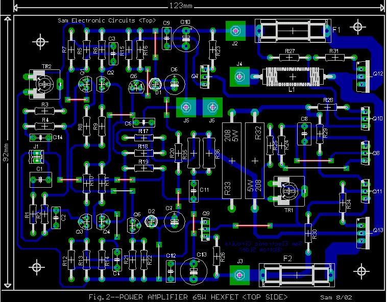
65W Power Amplifier PCB layout Electronic Schematic Diagram
Mini Amplifier with High Power Output Electronic Circuit

600 Watt Mosfet Power Amplifier Diagram with PCB Gallery Of Electronic Circuit Diagram Free

1000W Driver Power Amplifier Namec TEF Electronic Circuit

PCB Layout Design Image download Electronic Circuit

Marshal V.120PA Power Amplifier PCB Layout Electronic Circuit

500W RMS Power Amplifier Based MOSFET Schematic Design

500W Power Amplifier 2SC2922, 2SA1216 with PCB Layout Design Electronic Circuit

PCB Layout Design Image download Electronic Circuit

500W Power Amplifier 2SC2922, 2SA1216 with PCB Layout Design Electronic Circuit
